
ESD Protection Practice 3: Selection Guide and Layout Optimization Tips for Leiditech ESD Diodes
In the previous two articles, the Leiditech EMC guy talked about the hazards of ESD and the principle of protecting diodes. This time, the Leiditech EMC guy is back online, focusing on "practical operation”: How to select the right ESD protection diode for the protection circuit? What details can affect the protective effect when laying out a circuit board? The EMC guy from Leiditech has summarized a practical methodology of "selection + layout", which even beginners can quickly get started.
A、Three steps to select ESD protection diodes
The core of selection is "matching" - making the parameters of the diode precisely match the requirements of the protected circuit. Remember three key words: signal characteristics, protection requirements, and environmental tolerance.
Step 1: Match the signal characteristics
-
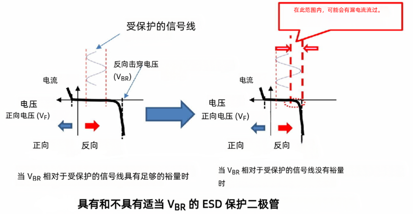
- Signal voltage: Focus on the "Maximum reverse operating Peak Voltage (VRWM)", which must be greater than or equal to the maximum voltage of the signal (for example, for a 5V signal line, select 5V or above for VRWM). If the VRWM is insufficient, the diode will leak electricity during normal operation, resulting in signal distortion.
- Signal frequency: For high-frequency signals (≥1GHz, such as USB 3.0), products with low capacitance values (CT≤1pF) must be selected; otherwise, insertion loss will increase. When CT > 1pF, the insertion loss of the USB 3.0 signal will exceed - 3dB@10GHz, which is prone to cause signal error. The low-capacity series of Leiditech Electronics (such as ULC0521CT) has only 0.18pF and is compatible with high-speed interfaces. At the same time, attention should be paid to the selection of packaging. For high-frequency or small-space scenarios, DFN packaging (parasitic inductance < 0.5nH) is preferred. For high-current scenarios, SOT-23FL packaging (with better heat dissipation performance) can be selected. Packaging parameters will indirectly affect the transmission of high-frequency signals and the long-term stability of the device.
- Signal voltage: Focus on the "Maximum reverse operating Peak Voltage (VRWM)", which must be greater than or equal to the maximum voltage of the signal (for example, for a 5V signal line, select 5V or above for VRWM). If the VRWM is insufficient, the diode will leak electricity during normal operation, resulting in signal distortion.
-
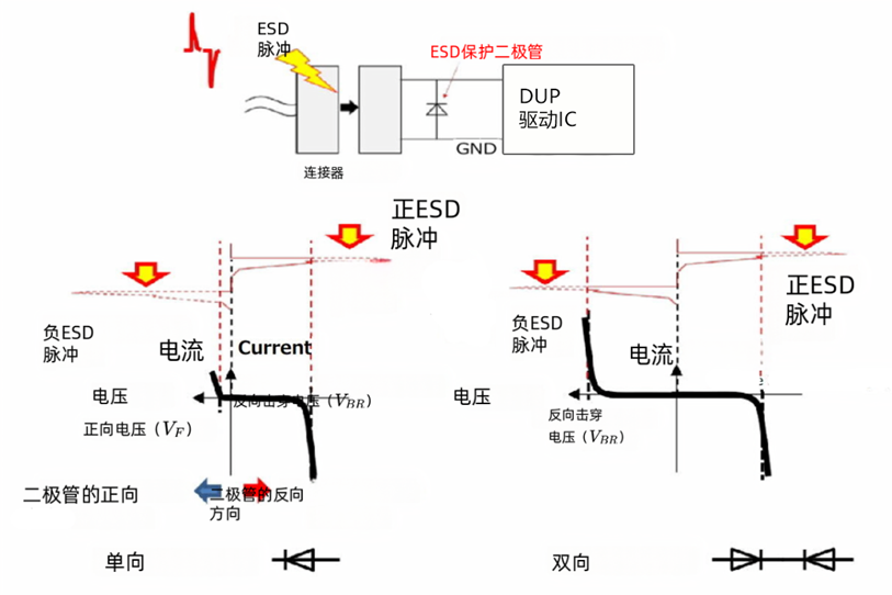
- Signal polarity: Unidirectional diodes are optional for unipolar signals (such as 0-5V digital signals). For bipolar signals (such as audio signals, ±12V power supply), select a bidirectional diode (Leiditech Electronics LCC05DT3 audio electrostatic protection).
Step 2: Meet the protection requirements
- ESD grade: Select according to the system test standard (such as IEC 61000-4-2 Contact Discharge ±8kV), and the VESD (Electrostatic Withstand Voltage) of the diode must be higher than this value. The VESD of the conventional part number of Leiditech Electronics can reach ±15kV, and that of the industrial-grade model can reach ±30kV.
- Clamping capability: ESD protection diodes do not respond immediately after electrostatic injection. If the first peak of the electrostatic pulse is higher than the clamping voltage of the ESD protection diode, this peak voltage may be applied to the protected device (DUP), causing it to malfunction or be damaged. Under the same current, the lower the clamping voltage (VC), the better. For example, for a 33V VRWM diode, under a 10A pulse, the VC of Leiditech’s part numbers is 5-8V lower than that of its competitors, which can better protect sensitive chips.
Step 3: Adapting to Environmental Tolerance
- Surge current: If the circuit may encounter lightning strikes or power surges (such as in outdoor equipment), attention should be paid to the "8/20μs peak pulse current (IPP)". The high-power part numbers of Leidtech Electronics can achieve an IPP of 100A, meeting the IEC 61000-4-5 test.
- Operating temperature: For industrial scenarios, choose wide-temperature products ranging from -55 ℃ to 150℃. The entire series of Leiditech Electronics meet industrial requirements.
B、Circuit board layout: Details determine the protective effect
Even after choosing the right part number, an improper layout may still cause the protection to fail. leiditech EMC guy summarized three "golden principles" :
- Signal polarity: Unidirectional diodes are optional for unipolar signals (such as 0-5V digital signals). For bipolar signals (such as audio signals, ±12V power supply), select a bidirectional diode (Leiditech Electronics LCC05DT3 audio electrostatic protection).

1. The diode must be "close to the ESD entry"
The high-frequency components of the ESD pulse will propagate along the "shortest path". If the diode is too far from the interface (for example, more than 5cm), the pulse will first break through the protected chip and then reach the diode. It is recommended that the trace length of the diode from the interface connector be no more than 3cm to further shorten the pulse propagation time.
The correct approach: The diode should be placed close to the USB, network port and other interfaces. The signal line should pass through the diode first and then reach the chip.
2. The grounding path should be "short, straight and thick
The ESD current of diode shunt needs to return to ground quickly. If there are many ground vias, thin wires, and long paths, "parasitic inductance" will be generated, causing the clamping voltage to rise (inductance × current change rate = additional voltage). Actual measurements show that when the spacing of grounding vias is greater than 5mm or the width of the ground line is less than 0.3mm, the parasitic inductance will increase by 2-3 NH, which in turn will cause the clamping voltage to rise by 10-15V, weakening the protective effect.
The correct approach: Connect the grounding terminal of the diode with copper coating, and drill ground vias nearby (preferably two or more), avoiding long and thin wires.
3. Avoid "parallel line interference"
ESD pulses generate strong electromagnetic fields around. If sensitive signal lines (such as I2C, SPI) run parallel to interface lines, high voltage will be induced.
The correct approach: The sensitive lines and interface lines should be arranged in a cross layout or isolated by ground lines, with a spacing of ≥3mm.
C、Recommendations for Leiditech selection tools
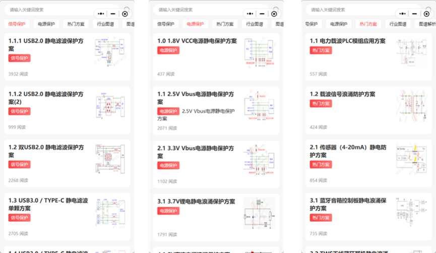
In order to simplify the selection, the official website of Shanghai Leiditech electronics (www.leiditech.com) provides the "parameter filtering tool", which can automatically match and adapt the part number by filtering the device power, operating voltage, package, clamping voltage; You can also search for the "EMC Electromagnetic Compatibility Community" mini-program created by Leiditech Electronics on wechat. It contains hundreds of reference design schemes for dozens of typical interfaces such as USB, HDMI, and Ethernet. The scheme content covers component selection, standard interpretation, and parameter comparison.
Summary
The core of selection is "parameter matching", and the core of layout is "shortening the path". If these two points are well done, the ESD protection effect can be improved by more than 80%.
Shanghai Leiditech Electronics is committed to becoming a leading brand in electromagnetic compatibility solutions and component supply, offering products such as ESD, TVS, TSS, GDT, MOV, MOSFET, Zener, inductors, etc. Leiditech has an experienced R&D team that can provide personalized customization services based on customer needs and offer the most superior solutions to customers.