
Rf antenna ESD protection multi-scheme design
EMC's ESD protection program for RF antennas is analyzed from two perspectives:
1. According to the frequency of different, in the case of ensuring the integrity of the signal, choose less than the ESD diode junction capacitance.
2. Select the ESD component corresponding to Vrwm (reverse working voltage) or slightly higher Vrwm according to the signal working peak voltage.
In this era of "intelligent connection of everything", mobile phone navigation, wireless headphones, smart home devices that we use every day are inseparable from an important component - radio frequency antenna. It is like the "signal transmitter" of electronic devices, which is responsible for converting our voice, video, and positioning information into electromagnetic waves and sending them out, while receiving wireless signals from all directions.
Different devices use different signal channels: the 700-3500MHz band used by mobile phone calls; The GPS system that the vehicle navigation relies on uses three dedicated frequency bands of 1175-1227MHz and 1575MHz; Bluetooth uses the 2.4 GHz frequency band, and Wi-Fi is mainly in 2.4 GHz, 5 GHz and 6GHz. When engineers design these antennas, they need to make the signal transmission stable, ensure that we don't brush video, navigation is not offset, and smart homes are always online.
Like static electricity when taking off a sweater, the antennas of mobile phones and smartwatches experience dozens of static "attacks" every day. These invisible electrostatic voltages are as high as thousands of volts, and as the wires get smaller and smaller, the precision circuits become fragile, and a single electrostatic shock can lead to failure. Designing anti-static protection for these precision antennas is the key to the reliability of the equipment.
To deal with the threat of static electricity, engineers have added TVS protective elements to the antenna. This miniature "safety valve" can be switched on instantly when electrostatic attack, releasing thousands of volts of current, avoiding damage to the core chip, so that the equipment can withstand the test of daily friction static electricity.
Select TVS We have to consider choosing the appropriate Vrwm ESD diode, RF signal power corresponding to the peak voltage is also different, so the choice of TVS operating voltage is also different. The following table shows the peak voltage corresponding to different RF signal powers when the impedance match is 50Ω.
|
RF Power(dBm)功率 |
Vrf(V)峰值电压 |
|
20 |
3.16 |
|
25 |
5.62 |
|
30 |
10.00 |
|
31 |
11.22 |
|
32 |
12.59 |
|
33 |
14.13 |
|
34 |
15.85 |
|
35 |
17.78 |
|
36 |
19.95 |
|
50Ω系统不同功率对应峰值电压 |
|
The VRWM (reverse operating voltage) used to match the antenna has a variety of voltages, from 1.0V to 24V can be selected.
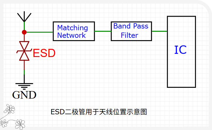
The main parameters of ESD diode parameter selection for antenna systems need to be concerned:
The VRWM voltage of the ESD diode must be higher than the peak voltage of the signal.
l ESD diode antistatic standards higher than customer requirements.
l According to the frequency, select ESD with low junction capacitance CJ to avoid affecting antenna transceiver signal distortion.
l Consider the RF signal receiving IC can withstand the voltage range, if the voltage is low, you can consider using ESD with Snapback (backscan), the test electrostatic protection is better.
The following list of ESD protection devices can be applied to different antenna signal interfaces:
|
Part Number |
|
|
VCmax@A |
C(PF) |
Features |
ESD per IEC61000-4-2 (Air)/(Contact) |
Package |
|
ULC0121CDN |
1.0 |
1.4 |
6V@4A |
0.35 |
1 CH.Bi. |
±15kV/±12kV |
DFN0603 |
|
ULC0142CDN |
1.0 |
4 |
6V@6A |
0.65 |
1 CH.Bi. |
±22kV/±20kV |
DFN1006 |
|
ULC01521CDN |
1.5 |
6 |
2.9V@4A |
0.2 |
1 CH.Bi. Snapback |
±15kV/±12kV |
DFN0603 |
|
ULC0321C13 |
3.3 |
5 |
15V@3A |
0.13 |
1 CH.Bi. |
±20kV/±20kV |
DFN0603 |
|
ULC0321CDNH |
3.3 |
4 |
5.5V@6A |
0.26 |
1 CH.Bi. Snapback |
|