
Leiditech ESD protection solution for PAD and stylus touch panels
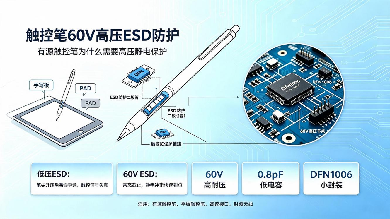
For PADs and active stylus pens, the pen tip is constantly in contact with the human hand and the screen, causing static electricity to build up easily. At the moment the pen tip touches the device, ESD pulses travel along the signal lines, impacting the touch controller IC, boost converter, and RF chips. At best, this causes touch malfunction; at worst, it can permanently damage components. Therefore, ESD protection diodes are essential protection components in the pen's internal circuit.
Hardware engineers and procurement personnel often have a common question during selection: ESD diodes are available in voltage ratings from 5V to over 100V. Why do active stylus pens with boost circuits require a 60V high-voltage model? If the voltage rating is too low, the device may false-trigger during normal operation, causing signal distortion. If the voltage rating is too high, it can degrade the high-frequency touch signal quality. This article uses the ULC6042C as an example to systematically analyze the design approach and selection specifications for high-voltage ESD protection in active stylus pens.
I.Why do PAD and active stylus pens require dedicated ESD protection diodes?
PAD and active stylus pen tips are constantly in contact with the human hand and the screen, easily generating thousands of volts of human-body ESD. Without protection, the transient high voltage directly strikes the touch controller chip and the boost circuit. The chip's transistors have weak voltage tolerance, and a single ESD strike can cause permanent damage, leading to issues such as touch discontinuities, stylus offset, and device recognition failure.
Conventional low-voltage ESD devices are prone to false triggering during normal operation. Ordinary high-voltage TVS devices have high junction capacitance, which attenuates high-frequency touch signals and reduces writing accuracy. A dedicated high-voltage ESD diode that matches the boost voltage, offers low capacitance, and comes in a small package is an essential component for active stylus pen circuit design.
II.Why does the active stylus pen tip circuit require a 60V ESD device like the ULC6042C?
PPAD and active stylus pens are powered by 3-4.2V lithium batteries, relying on an internal boost converter to raise the voltage to 20-50V to drive the pen tip antenna and generate electromagnetic signals for the screen digitizer to locate the pen position. Both mainstream solutions and high-end active pens use this high-voltage drive architecture, meaning the pen tip signal line normally operates at tens of volts for extended periods.
The key parameter of an ESD diode, the reverse working voltage VRWM, must be higher than the maximum operating voltage of the line. If the voltage rating is insufficient, the device may false-trigger during normal writing (without ESD), shunting the touch signal and causing pen drift, touch discontinuities, or even complete touch failure.
The ULC6042C has a reverse withstand voltage of 60V, fully covering the 20-50V pen tip operating voltage:
1. During normal writing, the diode remains stably reverse-biased, allowing the touch signal to transmit intact.
2. When the pen tip is subjected to ±8 to ±15kV human-body ESD, the device rapidly avalanches and conducts within nanoseconds, clamping and discharging the transient high voltage to ground, reliably protecting the downstream touch controller IC and boost circuit from breakdown.
III.Typical protection circuit architecture of the ULC6042C inside a stylus pen
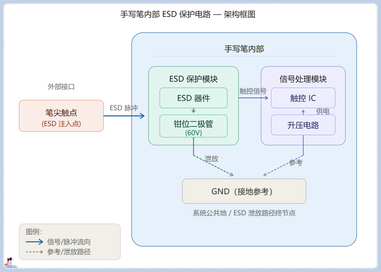 |
The ULC6042C is connected in parallel between the pen tip signal line and the system GND, installed at the location immediately behind the pen tip connector and before the touch controller IC. It serves as the first line of protection against ESD entering the PCB.
· Normal operation: Pen tip signal voltage < 60V, the diode remains off, and the high-frequency touch signal is transmitted intact.
· ESD event: The pen tip introduces a thousands-of-volts ESD pulse. The device rapidly conducts, discharging the transient high-voltage energy to the common ground plane, limiting the voltage seen by downstream chips to a safe clamping range.
IV.Key parameters and features of the ULC6042C
|
Parameters |
Specifications |
Description |
|
Package |
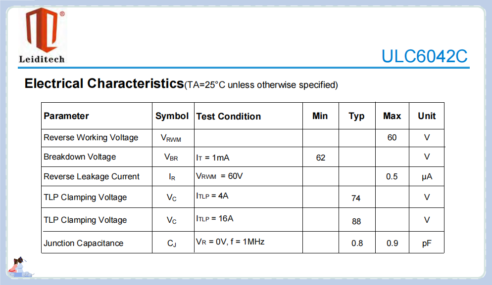
DFN1006 (1.0×0.6mm) |
Ultra-small leadless package, suitable for the extremely limited PCB space inside stylus pens |
|
Junction capacitance CJ |
0.8pF (typical) |
Low capacitance, suitable for high-frequency signal line protection without affecting touch sampling or Bluetooth communication |
|
Reverse working voltage VRWM |
60V |
Remains off during normal operation without false triggering |
|
Breakdown voltage VBR |
62V |
The threshold for rapid conduction during an ESD event |
|
TLP clamping voltage VC |
74V @ 4A – 88V @ 16A |
Clamps voltage within a safe range during an ESD event |
|
ESD protection level |
IEC 61000-4-2: Air ±20kV / Contact ±15kV |
Contact/air discharge protection capability |
|
Response time |
Nanosecond level (<1ns) |
Ensures response before the ESD rise time |
Product core advantages summary:
1. 60V high voltage rating: Matches the high-voltage nodes of active stylus pens, preventing false triggering during normal operation.
2. Ultra-low junction capacitance of 0.8pF: Does not attenuate high-frequency touch sampling or Bluetooth RF signals, ensuring writing accuracy and wireless communication stability.
3. DFN1006 ultra-small package (1.0×0.6mm): Extremely compact size, suitable for the constrained PCB layout space inside stylus pens.
4. Nanosecond-level ultra-fast response (<1ns): Conducts at the ESD pulse rise time, promptly clamping transient high voltage.
5. High ESD protection level: IEC 61000-4-2 compliant, with Air ±20kV and Contact ±15kV, meeting stringent consumer electronics ESD test requirements.
6. Low leakage current: Only 0.5μA leakage current at 60V rated voltage, preserving stylus pen battery life.
V.Selection criteria for ESD diodes in PAD and active stylus pens
The 60V ULC6042C is only suitable for active stylus pens with an internal boost converter and a pen tip operating voltage of 30–50V. It is not a universal solution for all stylus pens. Selection must be based on the maximum operating voltage of the pen tip line:
1. Scenarios requiring a 60V ESD diode:
Active stylus pens with an internal boost converter and a pen tip drive voltage of 30–50V. If a 24V/36V low-voltage ESD is used, the device will continuously conduct and shunt current during writing, directly causing touch failure。
2. Scenarios for 5–12V low-voltage ESD diodes:
Passive EMR electromagnetic pens (e.g., Wacom solution): no internal battery or boost converter; they rely on inductive coupling from the screen for power, and the pen tip voltage is extremely low. A low-voltage ESD is sufficient for protection.
3. Scenarios for 24V/36V medium-voltage ESD diodes:
Active pens with a low boost voltage specification, where the pen tip drive voltage is only 10–20V. A 60V device is not required, reducing BOM cost.
Core selection formula:
ESD diode VRWM (reverse working voltage) > maximum normal operating voltage of the pen tip signal line, with voltage margin.
· Pen tip operating voltage ≤ 5V: 5–12V series ESD
· Pen tip operating voltage 10–20V: 24V/36V series ESD
· Pen tip operating voltage 30–50V: 60V series ULC6042C
For 5–12V ESD used in stylus pens, these are standard parts for Shanghai Leiditech with multiple models available. Please contact the Leiditech EMC engineer.
For ESD devices with voltage ratings between 24V and 70V, commonly used models are listed in the table below:
|
Part No. 型号 |
Vrwm(V) 反向电压 |
Vb(V) 击穿电压 |
VCmax@A |
Cj(PF) 结电容 |
IEC61000-4-2 Air/Contact 静电 |
Features 单/双向 |
Package 封装 |
|
ULC2421CS |
24.0 |
30.0 |
6V@5A |
0.5 |
±15kV/±15kV |
Bidirectional |
DFN0603 (0201) |
|
ULC2442CS |
24.0 |
30.0 |
6V@5A |
0.5 |
±15kV/±15kV |
Bidirectional |
DFN1006 (0402) |
|
ULC3011CLV |
30.0 |
32.0 |
25V@12A |
0.7 |
±10kV/±10kV |
Bidirectional |
DFN1006 (0402) |
|
ULC3621CDN |
36.0 |
37.0 |
72V@16A |
0.3 |
±15kV/±8kV |
Bidirectional |
DFN0603 (0201) |
|
ULC3621CS |
36.0 |
44.0 |
8V@7A |
0.38 |
±14kV/±14kV |
Bidirectional |
DFN0603 (0201) |
|
ULC6042C |
60.0 |
62.0 |
88V@16A ITLP |
0.8 |
±20kV/±15kV |
Bidirectional |
DFN1006 (0402) |
|
ULC7042C |
70.0 |
80.0 |
100V@16A ITLP |
0.6 |
±10kV/±10kV |
Bidirectional |
DFN0603 (0201) |
VI.Main application scenarios of the ULC6042C
1. Core application: ESD protection for the pen tip signal line of active stylus pens and tablet styluses.
2. High-speed digital interfaces: ESD protection for high-speed differential signal lines in various devices.
3. RF circuits: ESD protection for Bluetooth, wireless antenna front-end ports.
4. Automotive electronics: ESD and surge suppression for ADAS sensors and in-vehicle communication interfaces.
5. Portable consumer electronics: Protection for GPIO, physical buttons, and micro-sensor interfaces in mobile phones and tablets.
VII.Application circuit design guidelines
1. Device placement: Place the ESD diode as close as possible to the pen tip connector, positioned as the first stage of ESD protection on the PCB, in front of the touch controller IC.
2. Ground routing guidelines: Use short, wide traces to connect the device's ground pad directly to the main ground plane, shortening the discharge path, reducing trace inductance, and improving ESD discharge efficiency.
3. Voltage matching principle: Strictly ensure that the device's VRWM is higher than the maximum normal operating voltage of the line, with a 5–10V voltage margin.
4. Signal integrity control: The ultra-low junction capacitance of 0.8pF prevents attenuation or phase shift of high-frequency touch signals, ensuring smooth, lag-free writing.
VIII.ULC6042C Datasheet Parameters
 |